Report: South Korean chipmaker chooses Indiana for cutting-edge plant
Subscriber Benefit
As a subscriber you can listen to articles at work, in the car, or while you work out. Subscribe Now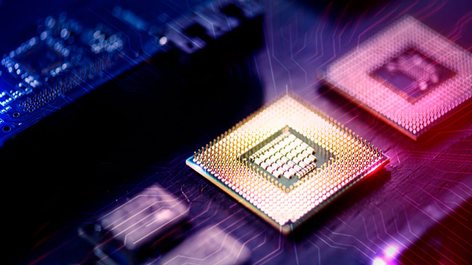
SK Hynix, a semiconductor chip maker based in South Korea, plans to build a cutting-edge packaging plant in Indiana, according to report Thursday in the Financial Times.
The move would give a boost to the U.S. Department of Commerce’s recently launched, $3 billion effort to stimulate the domestic chip-packaging industry.
The Indiana plant will be funded out of a $22 billion investment in the U.S. that was announced by the SK Group conglomerate’s chair Chey Tae-won during a public conference call with President Biden in 2022, according to the Financial Times report.
The location and cost of the plant are unclear. The Financial Times story is based on unnamed sources who have knowledge of the plan. Representatives of SK Hynix told FT that “our official position is that we are currently considering a possible investment in the US but haven’t made a final decision yet.”
A representative of the Indiana Economic Development Corp. told IBJ on Thursday that the agency would not comment about any specific developments.
“As semiconductor companies around the world consider North American location options, Indiana continues to become a global destination for this growing industry thanks to our highly skilled workforce, central location, strong communities and long-term partnership approach. Regarding specific projects, we are unable to confirm or comment, as all economic development negotiations are confidential,” said Erin Sweitzer, vice president of external communications for IEDC.
According to the Financial Times, SK Hynix is the world’s leading producer of high-bandwidth memory chips, crucial components in Silicon Valley giant Nvidia’s graphics processing units, which are used to train systems such as Open AI’s ChatGPT.
Packaging refers to the process of putting together individual chips for use in commercial products like phones and cars, as well as military applications including nuclear missiles. The Commerce Department says the U.S. has just 3% of the world’s packaging capacity—compared with an estimated 38% in China—which Washington worries has left the country vulnerable.
The U.S. packaging program is the first major research and development investment from the 2022 Chips and Science Act, which aims to revive semiconductor production in the U.S. as the development of critical electronic components has become a geopolitical battleground between the U.S. and China.